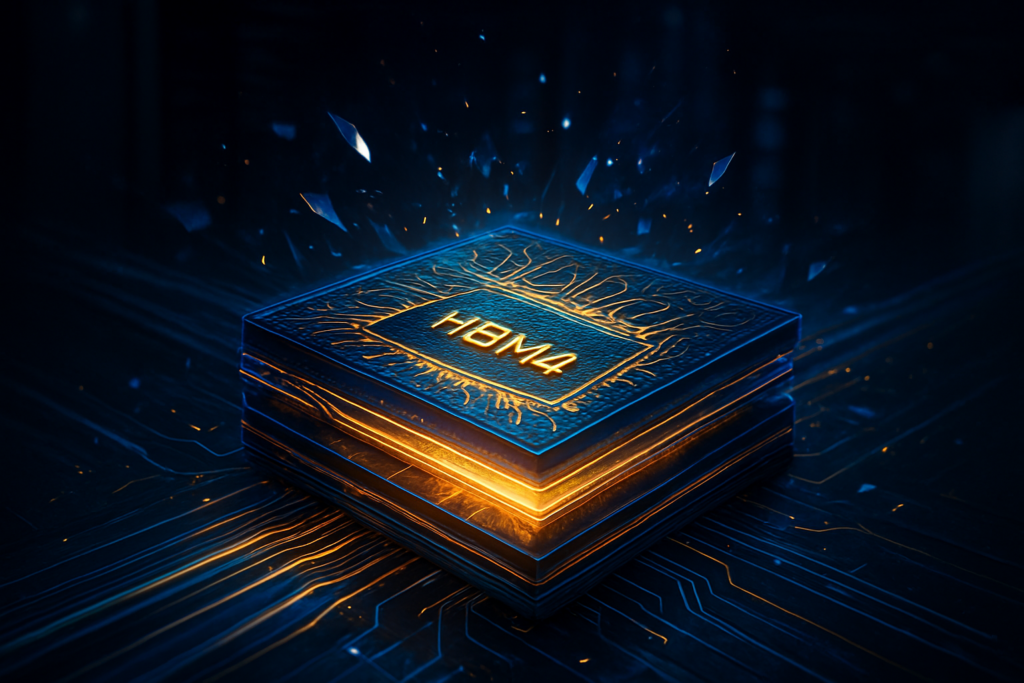
In a pivotal shift for the global semiconductor landscape, Samsung Electronics (KRX: 005930) has officially cleared final verification for its sixth-generation high-bandwidth memory, known as HBM4, for use in NVIDIA's (NASDAQ: NVDA) upcoming "Rubin" AI platform. This milestone, achieved in late January 2026, marks a dramatic resurgence for the South Korean tech giant after it spent much of the previous two years trailing behind competitors in the high-stakes AI memory race. With mass production scheduled to commence this month, Samsung has secured its position as a primary supplier for the hardware that will power the next era of generative AI.
The verification success is more than just a technical win; it is a strategic lifeline for the global AI supply chain. For over a year, NVIDIA and other AI chipmakers have faced bottlenecks due to the limited production capacity of previous-generation HBM3e memory. By bringing Samsung's HBM4 online ahead of the official Rubin volume rollout in the second half of 2026, NVIDIA has effectively diversified its supply base, reducing its reliance on a single provider and ensuring that the massive compute demands of future large language models (LLMs) can be met without the crippling shortages that characterized the Blackwell era.
The Technical Leap: 1c DRAM and the Turnkey Advantage
Samsung’s HBM4 represents a fundamental departure from the architecture of its predecessors. Unlike HBM3e, which focused primarily on incremental speed increases, HBM4 moves toward a logic-integrated architecture. Samsung’s specific implementation features 12-layer (12-Hi) stacks with a capacity of 36GB per stack. These modules utilize Samsung’s sixth-generation 10nm-class (1c) DRAM process, which reportedly offers a 20% improvement in power efficiency—a critical factor for data centers already struggling with the immense thermal and electrical requirements of modern AI clusters.
A key differentiator in Samsung's approach is its "turnkey" manufacturing model. While competitors often rely on external foundries for the base logic die, Samsung has leveraged its internal 4nm foundry process to produce the logic die that sits at the bottom of the HBM stack. This vertical integration allows for tighter coupling between the memory and logic components, reducing latency and optimizing the power-performance ratio. During testing, Samsung’s HBM4 achieved data transfer rates of 11.7 Gbps per pin, surpassing the JEDEC standard and providing a total bandwidth exceeding 2.8 TB/s per stack.
Industry experts have noted that this "one-roof" solution—encompassing DRAM production, logic die manufacturing, and advanced 2.5D/3D packaging—gives Samsung a unique advantage in shortening lead times. Initial reactions from the AI research community suggest that the integration of HBM4 into NVIDIA’s Rubin platform will enable a "memory-first" architecture, where the GPU is less constrained by data transfer bottlenecks, allowing for the training of models with trillions of parameters in significantly shorter timeframes.
Reshaping the Competitive Landscape: The Three-Way War
The verification of Samsung’s HBM4 has ignited a fierce three-way battle for dominance in the high-performance memory market. For the past two years, SK Hynix (KRX: 000660) held a commanding lead, having been the exclusive provider for much of NVIDIA’s early AI hardware. However, Samsung’s early leap into HBM4 mass production in February 2026 threatens that hegemony. While SK Hynix remains a formidable leader with its own HBM4 units expected later this year, the market share is rapidly shifting. Analysts estimate that Samsung could capture up to 30% of the HBM4 market by the end of 2026, up from its lower double-digit share during the HBM3e cycle.
For NVIDIA, the inclusion of Samsung is a tactical masterpiece. It places the GPU kingmaker in a position of maximum leverage over its suppliers, which also include Micron (NASDAQ: MU). Micron has been aggressively expanding its capacity with a $20 billion capital expenditure plan, aiming for a 20% market share by late 2026. This competitive pressure is expected to drive down the premiums associated with HBM, potentially lowering the overall cost of AI infrastructure for hyperscalers and startups alike.
Furthermore, the competitive dynamics are forcing new alliances. SK Hynix has deepened its partnership with Taiwan Semiconductor Manufacturing Co. (NYSE: TSM) to co-develop the logic dies for its version of HBM4, creating a "One-Team" front against Samsung’s internal foundry model. This divergence in strategy—integrated vs. collaborative—will be the defining theme of the semiconductor industry over the next 24 months as companies race to provide the most efficient "Custom HBM" solutions tailored to specific AI workloads.
Breaking the Memory Wall in the Rubin Era
The broader significance of Samsung’s HBM4 verification lies in its role as the engine for the NVIDIA Rubin architecture. Rubin is designed as a "sovereign AI" powerhouse, featuring the Vera CPU and Rubin GPU built on a 3nm process. Each Rubin GPU is expected to utilize eight stacks of HBM4, providing a staggering 288GB of high-speed memory per chip. This massive increase in memory capacity and bandwidth is the primary weapon in the industry's fight against the "Memory Wall"—the point where processor performance outstrips the ability of memory to feed it data.
In the global AI landscape, this breakthrough facilitates the move toward more complex, multi-modal AI systems that can process video, audio, and text simultaneously in real-time. It also addresses growing concerns regarding energy consumption. By utilizing the 1c DRAM process and advanced packaging, HBM4 delivers more "work per watt," which is essential for the sustainability of the massive data centers being planned by tech giants.
Comparisons are already being drawn to the 2023 transition to HBM3, which enabled the first wave of the generative AI boom. However, the shift to HBM4 is seen as more transformative because it signals the end of generic memory. We are entering an era of "Custom HBM," where the memory is no longer just a storage bin for data but an active participant in the compute process, with logic dies optimized for specific algorithms.
Future Horizons: 16-Layer Stacks and Hybrid Bonding
Looking ahead, the roadmap for HBM4 is already extending toward even denser configurations. While the current 12-layer stacks are the initial focus, Samsung is already conducting pilot runs for 16-layer (16-Hi) HBM4, which would increase capacity to 48GB or 64GB per stack. These future iterations are expected to employ "hybrid bonding" technology, a manufacturing technique that eliminates the need for traditional solder bumps between layers, allowing for thinner stacks and even higher interconnect density.
Experts predict that by 2027, the industry will see the first "HBM-on-Chip" designs, where the memory is bonded directly on top of the processor logic rather than adjacent to it. Challenges remain, particularly regarding the yield rates of these ultra-complex 3D structures and the precision required for hybrid bonding. However, the successful verification for the Rubin platform suggests that these hurdles are being cleared faster than many anticipated. Near-term applications will likely focus on high-end scientific simulation and the training of the next generation of "frontier models" by organizations like OpenAI and Anthropic.
A New Chapter for AI infrastructure
The successful verification of Samsung’s HBM4 for NVIDIA’s Rubin platform marks a definitive end to Samsung’s period of playing catch-up. By aligning its 1c DRAM and internal foundry capabilities, Samsung has not only secured its financial future in the AI era but has also provided the industry with the diversity of supply needed to maintain the current pace of AI innovation. The announcement sets the stage for a blockbuster GTC 2026 in March, where NVIDIA is expected to showcase the first live demonstrations of Rubin silicon powered by these new memory stacks.
As we move into the second half of 2026, the industry will be watching closely to see how quickly Samsung can scale its production to meet the expected deluge of orders. The "Memory Wall" has been pushed back once again, and with it, the boundaries of what artificial intelligence can achieve. The next few months will be critical as the first Rubin-based systems begin their journey from the assembly line to the world’s most powerful data centers, officially ushering in the sixth generation of high-bandwidth memory.
This content is intended for informational purposes only and represents analysis of current AI developments.
TokenRing AI delivers enterprise-grade solutions for multi-agent AI workflow orchestration, AI-powered development tools, and seamless remote collaboration platforms.
For more information, visit https://www.tokenring.ai/.


