
In a historic turning point for the global electronics industry, Japan has officially reclaimed its status as a top-tier semiconductor superpower. As of February 5, 2026, a series of strategic maneuvers by the Japanese government, anchored by massive subsidies and international partnerships, has successfully lured the world's most advanced manufacturing processes back to the archipelago. The crowning achievement of this "Silicon Renaissance" was confirmed today in Tokyo, as leadership from the Taiwan Semiconductor Manufacturing Company (TSMC) (NYSE: TSM) and the Japanese administration announced a radical upgrade to their joint venture in Kumamoto, securing the production of 3nm logic chips on Japanese soil.
This development is more than just an industrial expansion; it is a foundational pillar of Japan’s revised economic security strategy. By securing 3nm production at TSMC’s second Kumamoto facility and providing unprecedented state support for the domestic champion Rapidus, Japan is effectively insulating itself from the geopolitical instabilities of the Taiwan Strait while positioning its economy at the heart of the generative AI revolution. The move signals a definitive end to Japan's "lost decades" in semiconductor leadership, transitioning the nation from a supplier of legacy automotive chips to a global hub for the high-performance silicon required for next-generation AI and supercomputing.
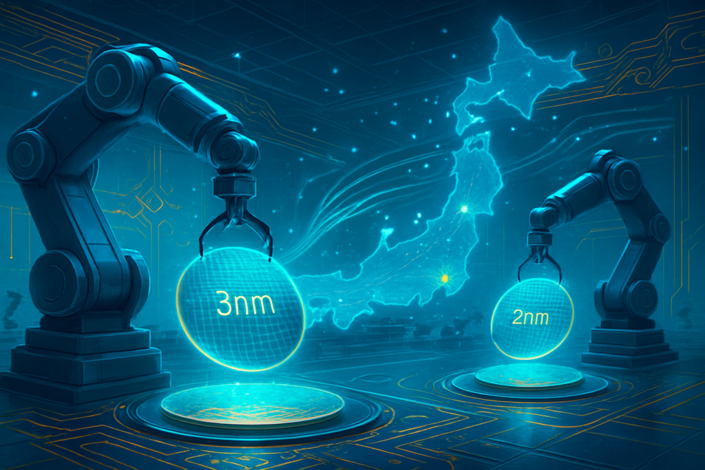
Technical Milestones: From 12nm to 2nm Logic
The technical specifications of Japan’s new semiconductor roadmap represent a quantum leap in domestic capabilities. The centerpiece of this transformation is the Japan Advanced Semiconductor Manufacturing (JASM) Fab 2 in Kumamoto. Initially conceived to produce 6nm and 12nm nodes, today’s announcement confirms that TSMC (NYSE: TSM) will instead deploy its ultra-advanced 3nm process technology at the site. This process utilizes FinFET (Fin Field-Effect Transistor) architecture refined to its absolute limit, offering significant improvements in power efficiency and transistor density over the 12nm to 28nm chips currently being produced at the adjacent Fab 1.
Simultaneously, the state-backed venture Rapidus is making rapid strides in Hokkaido with its "short Turnaround Time" (TAT) manufacturing model. Having successfully operationalized its 2nm pilot line in April 2025, Rapidus is currently utilizing the world’s most advanced High-NA EUV (Extreme Ultraviolet) lithography machines to refine its 2nm Gate-All-Around (GAA) transistor prototypes. This architecture differs fundamentally from previous FinFET designs by surrounding the channel on all four sides, significantly reducing current leakage and enabling the performance levels required for the next decade of AI acceleration.
The initial reactions from the global research community have been overwhelmingly positive, albeit marked by surprise at the speed of Japan's ascent. Analysts at major tech firms had previously doubted Rapidus’s ability to leapfrog multiple generations of technology, yet the delivery of the 2nm Process Design Kit (PDK) to early-access customers this month suggests the company is on track for its 2027 mass production goal. The shift in Kumamoto from 6nm to 3nm is being hailed by industry experts as a "strategic masterstroke" that provides Japan with immediate sovereign access to the chips powering the latest smartphones and data center GPUs.
Market Implications: Securing the AI Supply Chain
The implications for the global tech market are profound, creating a new competitive landscape for both established giants and emerging startups. Major Japanese corporations like Sony Group Corporation (NYSE: SONY) and Toyota Motor Corporation (NYSE: TM), both of which are investors in the Kumamoto project, stand to benefit immensely. For Sony, localized 3nm production ensures a stable supply of advanced logic for its world-leading image sensors and PlayStation ecosystem. For Toyota and its Tier-1 supplier Denso (TSE: 6902), the proximity of leading-edge logic is critical as vehicles transition into "computers on wheels" powered by autonomous driving AI.
This development also creates a significant strategic advantage for international players looking to diversify their supply chains. International Business Machines Corporation (NYSE: IBM), which has been a primary technology partner for Rapidus, now has a reliable path to bring its 2nm designs to market outside of the traditional foundry hubs. Meanwhile, AI powerhouses like NVIDIA (NASDAQ: NVDA) and SoftBank Group Corp. (TSE: 9984) are reportedly eyeing Japan as a high-security alternative for chip fabrication, potentially disrupting the existing duopoly of Taiwan and South Korea.
The disruption to the status quo is palpable. By offering massive subsidies—reaching nearly ¥10 trillion ($65 billion) through 2030—Japan is successfully competing with the U.S. CHIPS Act and European initiatives. This aggressive market positioning has forced a re-evaluation of global semiconductor logistics. Companies that once viewed Japan as a source for legacy parts are now re-tooling their long-term strategies to include Japanese "Giga-fabs" as primary nodes for their most sophisticated product lines.
Global Context: Economic Security and Industrial Policy
Looking at the wider significance, Japan’s strategy represents the most successful execution of industrial policy in the 21st century. It marks a shift from the era of globalized, cost-optimized supply chains to a "friend-shoring" model where economic security and regional stability dictate manufacturing locations. This fits into a broader trend of "techno-nationalism," where the ability to produce advanced silicon is viewed as essential to national sovereignty as energy or food security.
The resurgence of the "Silicon Island" in Kyushu (where Kumamoto is located) and the emergence of a "Silicon Forest" in Hokkaido are revitalizing regional economies that had been stagnant for years. However, this rapid expansion is not without its concerns. The sheer scale of the Kumamoto and Hokkaido projects has put immense pressure on local infrastructure, leading to a shortage of specialized engineers and driving up land prices. Environmental critics have also raised questions about the massive water and energy requirements of 2nm and 3nm fabs, prompting the government to invest heavily in green energy solutions to power these facilities.
Comparisons to previous milestones, such as Japan's dominance in the memory chip market in the 1980s, are inevitable. Unlike that era, however, the current revival is characterized by deep international integration rather than isolationist competition. The partnership with TSMC and the R&D collaboration with IBM demonstrate a collaborative approach to overcoming the physical limits of Moore’s Law, ensuring that Japan’s return to the top is sustainable and integrated into the global AI ecosystem.
Future Outlook: The Road to 1.4nm
As we look toward the future, the roadmap is clear. The next 18 to 24 months will be a period of intensive equipment installation and yield optimization. TSMC's Fab 2 in Kumamoto is expected to begin its equipment move-in phase later this year, with a target for mass production by late 2027. For Rapidus, the focus will be on the transition from its pilot line to the IIM-1 mass production facility in Chitose, with a parallel track for "Advanced Packaging" scheduled to begin trial production in April 2026.
Potential applications on the horizon include "on-device AI" that operates with zero latency, advanced robotics for Japan’s aging workforce, and breakthroughs in quantum computing materials. Experts predict that if Rapidus successfully hits its 2027 targets, Japan could capture up to 20% of the global market for leading-edge logic by the early 2030s. The next major challenge will be the move toward the 1.4nm node, for which R&D is already underway in collaboration with European research hub Imec.
A New Era for Japanese Silicon
In summary, Japan has successfully orchestrated a stunning comeback in the semiconductor sector. By securing 3nm production with TSMC and aggressively pursuing 2nm independence via Rapidus, the nation has solved two problems at once: it has modernized its industrial base and secured its technological future. The strategy of using state capital to de-risk massive private investment has proven to be a blueprint for other nations to follow.
This development will likely be remembered as a pivotal moment in AI history—the point when the "hardware bottleneck" was addressed through geographic diversification. In the coming months, the industry will be watching for the first 2nm test chips from Hokkaido and the groundbreaking ceremonies for the next phase of the Kumamoto expansion. Japan is no longer just a participant in the global chip race; it is once again setting the pace.
This content is intended for informational purposes only and represents analysis of current AI developments.
TokenRing AI delivers enterprise-grade solutions for multi-agent AI workflow orchestration, AI-powered development tools, and seamless remote collaboration platforms.
For more information, visit https://www.tokenring.ai/.