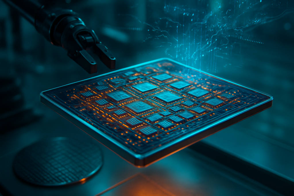
As the demand for generative AI training and inference reaches a fever pitch, the physical limits of semiconductor manufacturing are undergoing a radical transformation. Taiwan Semiconductor Manufacturing Co. (NYSE: TSM), the world’s most critical foundry, has officially initiated the transition to a revolutionary packaging architecture known as Chip-on-Panel-on-Substrate (CoPoS). This move marks the beginning of the end for the traditional 300mm circular silicon wafer as the primary medium for high-end AI chip assembly.
By shifting from the century-old circular wafer format to massive 12.2 x 12.2-inch rectangular panels, TSMC is effectively rewriting the rules of chip geometry. This development is not merely a matter of shape; it is a strategic maneuver designed to break through the "reticle limit"—the physical size boundary that has constrained chip designers for decades. The move to CoPoS promises to enable AI accelerators that are multiple times larger and significantly more powerful than anything on the market today, including the current industry-leading Blackwell architecture from Nvidia (NASDAQ: NVDA).
Redefining Geometry: The Technical Leap to 310mm Rectangular Panels
For over twenty years, the 300mm (12-inch) circular wafer has been the gold standard for semiconductor fabrication. However, for advanced packaging techniques like CoWoS (Chip-on-Wafer-on-Substrate), the circular shape is increasingly inefficient. When rectangular AI chips are placed onto a circular wafer, a significant portion of the area near the edges—often referred to as "edge loss"—is wasted. TSMC’s CoPoS technology addresses this by utilizing a 310mm x 310mm (12.2 x 12.2 inch) rectangular panel format. This shift alone increases area utilization from approximately 57% on a circular wafer to over 87% on a square panel, drastically reducing waste and manufacturing costs.
Beyond simple efficiency, CoPoS solves the looming "reticle limit" crisis. Traditional lithography machines are limited to exposing an area of roughly 858 square millimeters in a single pass. To create massive AI chips, manufacturers have had to "stitch" multiple reticle fields together on a silicon interposer. On a 300mm circular wafer, there is a physical ceiling to how many of these massive interposers can fit before hitting the curved edges. The CoPoS rectangular panel provides a vast, flat "backplane" that allows for interposers equivalent to 9.5 times the reticle limit. This allows for the integration of two or more 3nm compute dies alongside a staggering 12 to 16 stacks of High Bandwidth Memory (HBM4), a configuration that would be physically impossible to produce reliably on a circular wafer.
Initial reactions from the AI research community and hardware engineers have been overwhelmingly positive, though tempered by the technical hurdles of the transition. Integrating such large, complex systems on a single panel introduces significant "warpage" (bending) and thermal management challenges. However, recent reports from TSMC’s primary packaging partner, Xintec (TPE: 6239), indicate that trial yields for the 310mm pilot lines have already reached 90%. This success has cleared the way for TSMC to begin equipment validation for mass-scale production at its new AP7 facility in Chiayi, Taiwan.
The Nvidia Rubin Era and the Competitive Landscape
The immediate beneficiary of this packaging revolution is Nvidia, which has reportedly selected CoPoS as the foundational technology for its upcoming "Rubin" architecture. While the current Blackwell Ultra (B200/B300) series pushes the absolute limits of wafer-based CoWoS-L packaging, the Nvidia Rubin R100 and the Rubin Ultra—slated for late 2027 and 2028—require the massive real estate of rectangular panels to accommodate their unprecedented memory bandwidth and compute density. This "anchor tenancy" by Nvidia ensures that TSMC’s massive capital expenditure into CoPoS is de-risked by a guaranteed market for the high-end chips.
However, the shift to CoPoS is also a vital strategic move for other chip giants. Advanced Micro Devices (NASDAQ: AMD) and Broadcom (NASDAQ: AVGO) are reportedly in deep discussions with TSMC to utilize panel-level packaging for their future Instinct and custom AI silicon, respectively. For AMD, CoPoS offers a path to keep pace with Nvidia’s memory-heavy configurations, potentially allowing the future MI400 series to integrate even larger pools of HBM than previously thought possible. For Broadcom, the technology enables the creation of even more complex custom AI ASICs for hyperscalers like Google and Meta, who are desperate for larger "system-on-package" solutions to drive their next-generation large language models.
The competitive implications extend beyond the chip designers to the foundries themselves. By pioneering CoPoS, TSMC is widening the "moat" between itself and rivals like Samsung and Intel (NASDAQ: INTC). While Intel has been a proponent of glass substrate technology and advanced packaging via its EMIB and Foveros technologies, TSMC’s move to standardized large-format rectangular panels leverages existing supply chains from the display and PCB industries, potentially giving it a cost and scaling advantage that will be difficult for competitors to replicate in the near term.
A Fundamental Shift in the AI Scaling Paradigm
The move to CoPoS represents a significant milestone in the broader AI landscape, signaling a pivot from transistor-level scaling to "System-on-Package" scaling. As Moore’s Law—the doubling of transistors on a single die—becomes increasingly expensive and physically difficult to maintain, the industry is looking to advanced packaging to provide the next leap in performance. CoPoS is the ultimate expression of this trend, treating the package itself as the new platform for innovation rather than just a protective shell for the silicon.
This transition mirrors previous industry milestones, such as the shift from 200mm to 300mm wafers in the early 2000s, which radically lowered the cost of consumer electronics. However, the move to rectangular panels is arguably more significant because it changes the fundamental geometry of the semiconductor world to match the rectangular nature of the chips themselves. It also addresses environmental concerns by significantly reducing the amount of high-purity silicon wasted during the manufacturing process, a factor that is becoming increasingly important as the environmental footprint of AI infrastructure comes under scrutiny.
There are, however, potential concerns regarding the concentration of this technology. With the AP7 facility in Chiayi serving as the primary hub for CoPoS, the global AI supply chain remains heavily dependent on a single geographic location. This has led to intensified calls for TSMC to expand its advanced packaging capabilities globally. Recent rumors suggest that TSMC may eventually repurpose parts of its Arizona expansion for CoPoS by 2028, which would mark the first time such advanced rectangular packaging technology would be available on U.S. soil.
The Road Ahead: Glass Cores and the Feynman Generation
Looking toward the horizon, the 310mm rectangular panel is only the first step in TSMC’s long-term roadmap. By 2028 or 2029, experts predict a transition to even larger 515mm x 510mm panels. This will coincide with the introduction of "glass-core" substrates within the CoPoS framework. Glass offers superior flatness and thermal stability compared to organic materials, allowing for even tighter interconnect densities. This will likely be the cornerstone of Nvidia’s post-Rubin architecture, currently codenamed "Feynman."
The long-term development of CoPoS will also enable a new class of "megachips" that could power the first true Artificial General Intelligence (AGI) clusters. Instead of connecting thousands of individual chips via traditional networking, CoPoS may eventually allow for a "super-package" where dozens of compute dies and terabytes of HBM are integrated onto a single massive panel. The primary challenges remaining are the logistics of transporting such large, fragile panels and the development of new testing equipment that can handle the sheer scale of these components.
A New Foundation for AI History
The announcement and pilot-rollout of TSMC’s CoPoS technology in early 2026 marks a watershed moment for the semiconductor industry. It is a recognition that the circular wafer, while foundational to the first fifty years of computing, is no longer sufficient for the era of massive AI models. By embracing rectangular panel packaging, TSMC is providing the industry with the physical "runway" needed for AI accelerators to continue their exponential growth in capability.
The key takeaway for the coming weeks and months will be the progress of equipment installation at the AP7 facility and the finalized specifications for the HBM4 interface, which will be the primary cargo for these new rectangular panels. As we watch the first CoPoS chips emerge from the pilot lines, it is clear that the future of AI is no longer bound by the circle. The transition to the square is not just a change in shape—it is the birth of a new architecture for the intelligence of tomorrow.
This content is intended for informational purposes only and represents analysis of current AI developments.
TokenRing AI delivers enterprise-grade solutions for multi-agent AI workflow orchestration, AI-powered development tools, and seamless remote collaboration platforms.
For more information, visit https://www.tokenring.ai/.