
- Chiplet PHY simulator addresses the effects of forward clocking with single-ended signaling and higher bit error rate on die-to-die interconnect performance of chiplets
- Models and simulates UCIe-based compliance measures such as voltage transfer function
- Leverages Keysight EDA’s technology and history of success simulating complex physical layer standards such as SerDes and memory
Keysight Technologies, Inc. (NYSE: KEYS) introduces Chiplet PHY Designer, the latest member in its family of high speed digital design and simulation tools that provides die-to-die (D2D) interconnect simulation, which is a key step in verifying performance for heterogeneous and 3D integrated circuit (IC) designs commonly referred to as chiplets. The new electronic design automation (EDA) tool is the industry’s first to provide in-depth modeling and simulation capabilities that enable chiplet designers to rapidly and accurately verify that their designs meet specifications of the Universal Chiplet Interconnect Express™ (UCIe™) standard.
This press release features multimedia. View the full release here: https://www.businesswire.com/news/home/20240124811619/en/
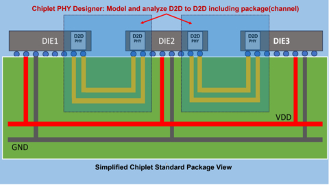
Chiplet PHY Designer simulates the UCIe specification for D2D physical layer interconnect. (Graphic: Business Wire)
UCIe is emerging as the leading chiplet interconnect specification in the semiconductor industry. It is an open standard that defines the interconnect between chiplets within an advanced 2.5D or 3D package. UCIe is in process of being supported or adopted by many of the top semiconductor equipment and EDA tool vendors as well as foundries and chiplet designers. Designers who use the interconnect standard and ensure their chiplets perform to its specifications are helping establish a broad ecosystem for chiplet interoperability and commerce.
Keysight EDA’s research and development team has been working on modeling and simulating high-speed digital interfaces aligned with industry specifications for decades. For example, ADS Memory Designer offers comprehensive memory interface coverage such as GDDR7, DDR5, LPDDR5, and HBM3 with its IBIS-AMI modeler. Its rigorous and genuine JEDEC compliance test solution handles over 100 test IDs with the same test algorithm found in the Keysight Infinium oscilloscope family.
Key features of the Chiplet PHY Designer physical-layer simulator include:
- Supports UCIe physical layer standard – automated parsing of signals following the standard naming conventions, automated connections between multiple dies through package interconnects, standard driven simulation setup such as speed grade, and intuitive measurement setup through specialized probe component.
- Measurement of voltage transfer function (VTF) – precisely computes a VTF to ensure UCIe specification compliance and analyzes system bit error rate (BER) down to 1e-27 or 1e-32 levels. Measures eye diagram height, eye width, skew, mask margin, and BER contour.
- Analysis of forwarded clocking to accurately capture the asynchronous clocking behavior.
Adrien Auge, Senior Staff Applications Engineer, Alphawave Semi, said: “The ability to validate Alphawave Semi’s chiplet solutions is crucial for enabling a future of heterogenous chip design, as it ensures seamless operation and interoperability for 2.5D/3D solutions available to our customers. Chiplet PHY Designer simplifies the electrical simulation process for large die-die electrical connectivity, such as UCIe. It provides engineers and designers a quick and easy path to extract electrical compliance of their solutions against the latest revision of the specification. Furthermore, by complying with the latest IBIS modeling specification for electrical I/O, physical integrators can delve deeper into the chiplet electrical validation process, leveraging our detailed models to obtain pre-silicon performance predictions.”
Niels Faché, Vice President and General Manager, Keysight EDA, said: “Our high-speed digital simulation team capitalized on its understanding of the shift left challenges presented by SerDes PHYS. They have applied these learnings to the chiplet domain to extend success of our standards-based simulation strategy to UCIe. Interconnect modeling is critical to system design and performance. Chiplet PHY Designer accelerates validation of chiplet subsystems, from one D2D PHY through interconnect channels to another D2D PHY, much earlier in the design cycle. It enables 3D IC designers to solve critical interconnect performance problems improving predictive virtual prototyping to speed time-to-market.”
See Chiplet PHY Designer at DesignCon
Keysight will be demonstrating Chiplet PHY Designer in its DesignCon booth #1039 at the Santa Clara Convention Center from January 31-February 1, 2024.
For more information, visit: Chiplet PHY Designer
About Keysight Technologies
At Keysight (NYSE: KEYS), we inspire and empower innovators to bring world-changing technologies to life. As an S&P 500 company, we’re delivering market-leading design, emulation, and test solutions to help engineers develop and deploy faster, with less risk, throughout the entire product lifecycle. We’re a global innovation partner enabling customers in communications, industrial automation, aerospace and defense, automotive, semiconductor, and general electronics markets to accelerate innovation to connect and secure the world. Learn more at Keysight Newsroom and www.keysight.com.
View source version on businesswire.com: https://www.businesswire.com/news/home/20240124811619/en/
Contacts
Keysight Media Contacts
Paul Erwin
Americas
+1 248 430–9075
paul.erwin@keysight.com
Fusako Dohi
Asia
+81 42 660-2162
fusako_dohi@keysight.com
Jenny Gallacher
Europe
+44 (0) 7800 737 982
jenny.gallacher@keysight.com