
In a definitive moment for the American semiconductor industry, Intel (NASDAQ: INTC) has officially transitioned its 18A (1.8nm-class) process node into high-volume manufacturing (HVM). The announcement, made early this month, signals the culmination of CEO Pat Gelsinger’s ambitious "five nodes in four years" roadmap, positioning Intel at the absolute bleeding edge of transistor density and power efficiency. This milestone is punctuated by the overwhelming critical success of the newly launched Panther Lake processors, which have set a new high-water mark for integrated AI performance and power-to-performance ratios in the mobile and desktop segments.
The shift represents more than just a technical achievement; it marks Intel’s full-scale re-entry into the foundry race as a formidable peer to Taiwan Semiconductor Manufacturing Company (NYSE: TSM). With 18A yields now stabilized above the 60% threshold—a key metric for commercial profitability—Intel is aggressively pivoting its strategic focus toward the upcoming 14A node and the massive "Silicon Heartland" project in Ohio. This pivot underscores a new era of silicon sovereignty and high-performance computing that aims to redefine the AI landscape for the remainder of the decade.
Technical Mastery: RibbonFET, PowerVia, and the Panther Lake Powerhouse
The move to 18A introduces two foundational architectural shifts that differentiate it from any previous Intel manufacturing process. The first is RibbonFET, Intel’s implementation of Gate-All-Around (GAA) transistor architecture. By surrounding the channel with the gate on all four sides, RibbonFET significantly reduces current leakage and improves electrostatic control, allowing for higher drive currents at lower voltages. This is paired with PowerVia, the industry’s first large-scale implementation of backside power delivery. By moving power routing to the back of the wafer and leaving the front exclusively for signal routing, Intel has achieved a 15% improvement in clock frequency and a roughly 25% reduction in power consumption, solving long-standing congestion issues in advanced chip design.
The real-world manifestation of these technologies is the Core Ultra Series 3, codenamed Panther Lake. Debuted at CES 2026 and set for global retail availability on January 27, Panther Lake has already stunned reviewers with its Xe3 "Célere" graphics architecture and the NPU 5. Initial benchmarks show the integrated Arc B390 GPU delivering up to 77% faster gaming performance than its predecessor, effectively rendering mid-range discrete GPUs obsolete for most users. More importantly for the AI era, the system’s total AI throughput reaches a staggering 120 TOPS (Tera Operations Per Second). This is achieved through a massive expansion of the Neural Processing Unit (NPU), which handles complex generative AI tasks locally with a fraction of the power required by previous generations.
A New Order in the Foundry Ecosystem
The successful ramp of 18A is sending ripples through the broader tech industry, specifically targeting the dominance of traditional foundry leaders. While Intel remains its own best customer, the 18A node has already attracted high-profile "anchor" clients. Microsoft (NASDAQ: MSFT) and Amazon (NASDAQ: AMZN) have reportedly finalized designs for custom AI accelerators and server chips built on 18A, seeking to reduce their reliance on external providers and optimize their data center overhead. Even more telling are reports that Apple (NASDAQ: AAPL) has qualified 18A for select future components, signaling a potential diversification of its supply chain away from its exclusive reliance on TSMC.
This development places Intel in a strategic position to disrupt the existing AI silicon market. By offering a domestic, leading-edge alternative for high-performance chips, Intel Foundry is capitalizing on the global push for supply chain resilience. For startups and smaller AI labs, the availability of 18A design kits means faster access to hardware that can run massive localized models. Intel's ability to integrate PowerVia ahead of its competitors gives it a temporary but significant "power-efficiency moat," making it an attractive partner for companies building the next generation of power-hungry AI edge devices and autonomous systems.
The Geopolitical and Industrial Significance of the 18A Era
Intel’s achievement is being viewed by many as a successful validation of the U.S. CHIPS and Science Act. With the Department of Commerce maintaining a vested interest in Intel’s success, the 18A milestone is a point of national pride and economic security. In the broader AI landscape, this move ensures that the hardware layer of the AI stack—which has been a significant bottleneck over the last three years—now has a secondary, highly advanced production lane. This reduces the risk of global shortages that previously hampered the deployment of large language models and real-world AI applications.
However, the path has not been without its concerns. Critics point to the immense capital expenditure required to maintain this pace, which has strained Intel's balance sheet and necessitated a highly disciplined "foundry-first" corporate restructuring. When compared to previous milestones, such as the transition to FinFET or the introduction of EUV (Extreme Ultraviolet) lithography, 18A stands out because of the simultaneous introduction of two radically new technologies (RibbonFET and PowerVia). This "double-jump" was considered high-risk, but its success confirms that Intel has regained its engineering mojo, providing a necessary counterbalance to the concentrated production power in East Asia.
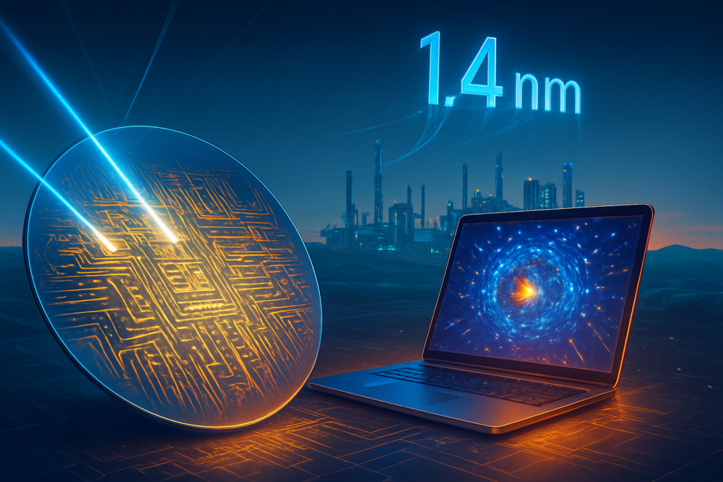
The Horizon: 14A and the Ohio Silicon Heartland
With 18A in mass production, Intel’s leadership has already turned their sights toward the 14A (1.4nm-class) node. Slated for production readiness in 2027, 14A will be the first node to fully utilize High-NA EUV lithography at scale. Intel has already begun distributing early Process Design Kits (PDKs) for 14A to key partners, signaling that the company does not intend to let its momentum stall. Experts predict that 14A will offer yet another 15-20% leap in performance-per-watt, further solidifying the AI PC as the standard for enterprise and consumer computing.
Parallel to this technical roadmap is the massive infrastructure push in New Albany, Ohio. The "Ohio One" project, often called the Silicon Heartland, is making steady progress. While initial production was delayed from 2025, the latest reports from the site indicate that the first two modules (Mod 1 and Mod 2) are on track for physical completion by late 2026. This facility is expected to become the primary hub for Intel’s 14A and beyond, with full-scale chip production anticipated to begin in the 2028 window. The project has become a massive employment engine, with thousands of construction and engineering professionals currently working to finalize the state-of-the-art cleanrooms required for sub-2nm manufacturing.
Summary of a Landmark Achievement
Intel's successful mass production of 18A and the triumph of Panther Lake represent a historic pivot for the semiconductor giant. The company has moved from a period of self-described "stagnation" to reclaiming a seat at the head of the manufacturing table. The key takeaways for the industry are clear: Intel’s RibbonFET and PowerVia are the new benchmarks for efficiency, and the "AI PC" has moved from a marketing buzzword to a high-performance reality with 120 TOPS of local compute power.
As we move deeper into 2026, the tech world will be watching the delivery of Panther Lake systems to consumers and the first batch of third-party 18A chips. The significance of this development in AI history cannot be overstated—it provides the physical foundation upon which the next decade of software innovation will be built. For Intel, the challenge now lies in maintaining this relentless execution as they break ground on the 14A era and bring the Ohio foundry online to secure the future of global silicon production.
This content is intended for informational purposes only and represents analysis of current AI developments.
TokenRing AI delivers enterprise-grade solutions for multi-agent AI workflow orchestration, AI-powered development tools, and seamless remote collaboration platforms.
For more information, visit https://www.tokenring.ai/.