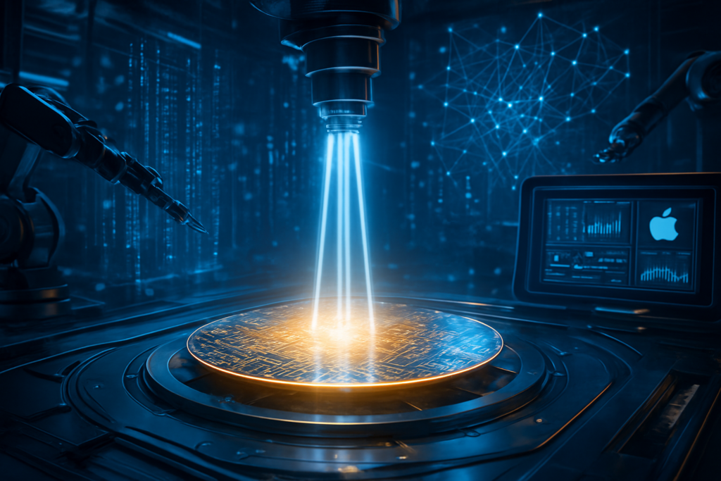
In a historic reversal of fortunes, Intel Corporation (NASDAQ: INTC) has officially reclaimed its position as a leading-edge semiconductor manufacturer. The company announced today that its 18A (1.8nm-class) process node has reached high-volume manufacturing (HVM) with stable yields surpassing the 60% threshold. This achievement marks the definitive completion of CEO Pat Gelsinger’s ambitious "Five Nodes in Four Years" (5N4Y) roadmap, a feat once thought impossible by many industry analysts.
The milestone is amplified by a stunning strategic shift from Apple (NASDAQ: AAPL), which has reportedly qualified the 18A process for its future M-series chips. This landmark agreement represents the first time Apple has moved to diversify its silicon supply chain away from its near-exclusive reliance on Taiwan Semiconductor Manufacturing Company (NYSE: TSM). By securing Intel as a domestic foundry partner, Apple is positioning itself to mitigate geopolitical risks while tapping into some of the most advanced transistor architectures ever conceived.
The Intel 18A process is more than just a reduction in size; it represents a fundamental architectural shift in how semiconductors are built. At the heart of this milestone are two key technologies: RibbonFET and PowerVia. RibbonFET is Intel’s implementation of Gate-All-Around (GAA) transistor architecture, which replaces the long-standing FinFET structure. By surrounding the transistor channel with the gate on all four sides, RibbonFET allows for precise electrical control, significantly reducing current leakage and enabling higher drive currents at lower voltages.
Equally revolutionary is PowerVia, Intel’s industry-first implementation of backside power delivery. Traditionally, power and signal lines are crowded together on the front of a wafer, leading to interference and efficiency losses. PowerVia moves the power delivery network to the back of the silicon, separating it from the signal wiring. Early data from the 18A HVM ramp indicates that this separation has reduced voltage droop by up to 30%, translating into a 5-10% improvement in logic density and a massive leap in performance-per-watt.
Industry experts and the research community have reacted with cautious optimism, noting that while TSMC’s upcoming N2 node remains slightly denser in terms of raw transistor count per square millimeter, Intel’s 18A currently holds a performance edge. This is largely attributed to Intel being the first to market with backside power, a feature TSMC is not expected to implement until its N2P or A16 nodes later in 2026 or 2027. The successful 60% yield rate is particularly impressive, suggesting that Intel has finally overcome the manufacturing hurdles that plagued its 10nm and 7nm transitions years ago.
The news of Apple qualifying 18A for its M-series chips has sent shockwaves through the technology sector. For over a decade, TSMC (NYSE: TSM) has been the sole provider for Apple’s custom silicon, creating a dependency that many viewed as a single point of failure. By integrating Intel Foundry Services (IFS) into its roadmap, Apple is not only gaining leverage in pricing but also securing a "geopolitical safety net" by utilizing Intel’s expanding fab footprint in Arizona and Ohio.
Apple isn't the only giant making the move. Recent reports indicate that Nvidia (NASDAQ: NVDA) has signed a strategic alliance worth an estimated $5 billion to secure 18A capacity for its next-generation AI architectures. This move suggests that the AI-driven demand for high-performance silicon is outstripping even TSMC’s massive capacity. Furthermore, hyperscale providers like Microsoft (NASDAQ: MSFT) and Amazon (NASDAQ: AMZN) have already confirmed plans to migrate their custom AI accelerators—Maia and Trainium—to the 18A node to take advantage of the PowerVia efficiency gains.
This shift positions Intel as a formidable "Western alternative" to the Asian manufacturing hubs. For startups and smaller AI labs, the availability of a high-performance, domestic foundry could lower the barriers to entry for custom silicon design. The competitive pressure on TSMC and Samsung (KRX: 005930) is now higher than ever, as Intel’s ability to execute on its roadmap has restored confidence in its foundry services' reliability.
Intel’s success with 18A is being viewed through a wider lens than just corporate profit; it is a major milestone for national security and the global "Silicon Shield." As AI becomes the defining technology of the decade, the ability to manufacture the world’s most advanced chips on American soil has become a strategic priority. The completion of the 5N4Y roadmap validates the billions of dollars in subsidies provided via the CHIPS and Science Act, proving that domestic high-tech manufacturing can remain competitive at the leading edge.
In the broader AI landscape, the 18A node arrives at a critical juncture. The transition from large language models (LLMs) to more complex multimodal and agentic AI systems requires exponential increases in compute density. The performance-per-watt benefits of 18A will likely define the next generation of data center hardware, potentially slowing the skyrocketing energy costs associated with massive AI training clusters.
This breakthrough also serves as a comparison point to previous milestones like the introduction of Extreme Ultraviolet (EUV) lithography. While EUV was the tool that allowed the industry to keep shrinking, RibbonFET and PowerVia are the architectural evolutions that allow those smaller transistors to actually function efficiently. Intel has successfully navigated the transition from being a "troubled legacy player" to an "innovative foundry leader," reshaping the narrative of the semiconductor industry for the latter half of the 2020s.
With the 18A milestone cleared, Intel is already looking toward the horizon. The company has teased the first "risk production" of its 14A (1.4nm-class) node, scheduled for late 2026. This next step will involve the first commercial use of High-NA EUV scanners—the most advanced and expensive manufacturing tools in history—produced by ASML (NASDAQ: ASML). These machines will allow for even finer resolution, potentially pushing Intel further ahead of its rivals in the density race.
However, challenges remain. Scaling HVM to meet the massive demands of Apple and Nvidia simultaneously will test Intel’s logistics and supply chain like never before. There are also concerns regarding the long-term sustainability of the high yields as designs become increasingly complex. Experts predict that the next two years will be a period of intense "packaging wars," where technologies like Intel’s Foveros and TSMC’s CoWoS (Chip on Wafer on Substrate) will become as important as the transistor nodes themselves in determining final chip performance.
The industry will also be watching to see how TSMC responds. With Apple diversifying, TSMC may accelerate its own backside power delivery (BSPD) roadmap or offer more aggressive pricing to maintain its dominance. The "foundry wars" are officially in high gear, and for the first time in a decade, it is a three-way race between Intel, TSMC, and Samsung.
The high-volume production of Intel 18A and the landmark deal with Apple represent a "Silicon Renaissance." Intel has not only met its technical goals but has also reclaimed the strategic initiative in the foundry market. The summary of this development is clear: the era of TSMC’s total dominance in leading-edge manufacturing is over, and a new, more competitive multi-source environment has arrived.
The significance of this moment in AI history cannot be overstated. By providing a high-performance, domestic manufacturing base for the chips that power AI, Intel is securing the infrastructure of the future. The long-term impact will likely be seen in a more resilient global supply chain and a faster cadence of AI hardware innovation.
In the coming weeks and months, the tech world will be watching for the first third-party benchmarks of 18A-based hardware and further announcements regarding the build-out of Intel’s "system foundry" ecosystem. For now, Pat Gelsinger’s gamble appears to have paid off, setting the stage for a new decade of semiconductor leadership.
This content is intended for informational purposes only and represents analysis of current AI developments.
TokenRing AI delivers enterprise-grade solutions for multi-agent AI workflow orchestration, AI-powered development tools, and seamless remote collaboration platforms.
For more information, visit https://www.tokenring.ai/.


