Boardman Bay Capital Management leads round joined by strategic investments from industry bellwethers Hewlett Packard Enterprise and NVIDIA, fast-tracking Ayar Labs’ transformational technology for AI, HPC, cloud, and telecom applications
Ayar Labs, the leader in chip-to-chip optical connectivity, today announced that the company has secured $130 million in additional financing led by Boardman Bay Capital Management to drive the commercialization of its breakthrough optical I/O solution. Hewlett Packard Enterprise (HPE) and NVIDIA entered this investment round, joining existing strategic investors Applied Ventures LLC, GlobalFoundries, Intel Capital, and Lockheed Martin Ventures. Other new strategic and financial investors participating in the round include Agave SPV, Atreides Capital, Berkeley Frontier Fund, IAG Capital Partners, Infinitum Capital, Nautilus Venture Partners, and Tyche Partners. They join existing investors such as BlueSky Capital, Founders Fund, Playground Global, and TechU Venture Partners.
This press release features multimedia. View the full release here: https://www.businesswire.com/news/home/20220426005529/en/
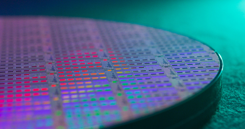
300mm wafer of Ayar Labs TeraPHY™ optical I/O chiplets (Photo: Business Wire)
“As a successful technology-focused crossover fund operating for over a decade, Ayar Labs represents our largest private investment to date," said Will Graves, Chief Investment Officer at Boardman Bay Capital Management. "We believe that silicon photonics-based optical interconnects in the data center and telecommunications markets represent a massive new opportunity and that Ayar Labs is the leader in this emerging space with proven technology, a fantastic team, and the right ecosystem partners and strategy.”
“Optical connectivity will be important to scale accelerated computing clusters to meet the fast-growing demands of AI and HPC workloads,” said Bill Dally, Chief Scientist and Senior Vice President of Research at NVIDIA. “Ayar Labs has unique optical I/O technology that meets the needs of scaling next-generation silicon photonics-based architectures for AI.”
Ayar Labs’ optical I/O solution eliminates the bottlenecks associated with system bandwidth, power consumption, latency, and reach, dramatically improving existing system architectures and enabling new, previously unrealizable solutions for artificial intelligence (AI), high performance computing (HPC), cloud, telecommunications, aerospace, and remote sensing applications. With the new investment, Ayar Labs is ramping production and securing supply chain partners, as signaled by previously announced multi-year strategic collaborations with Lumentum and Macom, both leaders in optical and photonic products, as well as GlobalFoundries on its new GF Fotonix™ platform.
“Ayar Labs’ highly differentiated technology is crucial to supporting the high-performance computing architectures of the future,” said Paul Glaser, Vice President and Head of Hewlett Packard Pathfinder, HPE’s venture arm. “Ayar Labs represents a strategic investment opportunity for HPE to help our customers more efficiently derive greater insights and value from their data.”
“The overall financing is much larger than we originally targeted, underscoring the market opportunity for optical I/O and Ayar Labs’ leadership position in silicon photonics-based interconnect solutions,” said Charles Wuischpard, CEO of Ayar Labs. “This financing allows us to fully qualify our solution against industry standards for quality and reliability and scale production starting this year.”
Ayar Labs also announced that it made its first volume commercial shipments under contract and expects to ship thousands of units of its in-package optical interconnect by end of year.
About Ayar Labs
Ayar Labs is disrupting the traditional performance, cost, and efficiency curves of the semiconductor and computing industries by driving a 1000x improvement in interconnect bandwidth density at 10x lower power. Ayar Labs’ patented approach uses industry standard cost-effective silicon processing techniques to develop high speed, high density, low power optical based interconnect “chiplets” and lasers to replace traditional electrical-based I/O. The company was founded in 2015 and is funded by a number of domestic and international Venture Capital firms as well as strategic investors. For more information, please visit http://www.ayarlabs.com.
About Boardman Bay
Boardman Bay Capital Management is an asset manager focused exclusively on the technology sector. With deep technology industry experience as both an operator and an investor, Boardman Bay has invested across public and private technology markets for the past decade. Since 2018, Boardman Bay has invested in a uniquely dedicated strategy that focuses on optical and “hard technology” companies as a new wave of innovation transforms data centers and global technology infrastructure. Boardman Bay manages venture and public equity funds while striving to be an expert partner to companies as they prepare for their next phase of transformational growth.
View source version on businesswire.com: https://www.businesswire.com/news/home/20220426005529/en/
Contacts
Kristine Raabe, press@ayarlabs.com